

Analog Layout Design
- Home

- Services
- Analog Layout Design
Layout Design
Our layout engineering team delivers high-quality physical implementations across a wide range of semiconductor process technologies. With strong expertise across both mature and advanced nodes, we support designs that demand high reliability, performance, and manufacturability.
Our Expertise
Technology Node Expertise
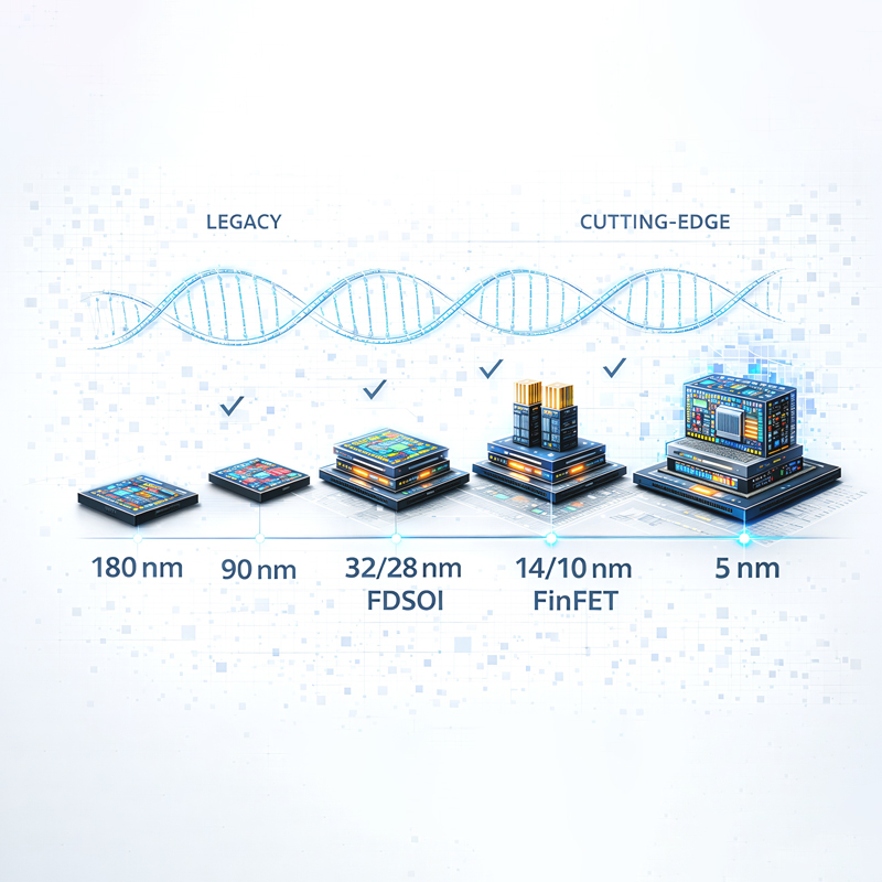
Our team brings proven expertise across a wide range of semiconductor technologies, from mature planar nodes (180 nm–40 nm) to advanced 28/32 nm FDSOI and cutting-edge FinFET nodes (14 nm to 2 nm). This breadth of experience enables us to seamlessly adapt to diverse process requirements and design challenges, delivering high-quality, optimized solutions across performance, power, and area (PPA) targets with speed and confidence.
Foundry Ecosystem Experience
We have strong familiarity with the design rules, layout methodologies, and verification flows of leading semiconductor foundries. Our engineers have delivered layouts across multiple industry platforms including TSMC, Intel, Texas Instruments, GlobalFoundries, Samsung, and ST-IBM FDSOI technologies. This experience ensures smooth collaboration with client teams and efficient preparation for fabrication.

Full-Chip Layout & Integration
Beyond individual blocks, we provide expertise in full-chip physical implementation. Our capabilities include chip-level floorplanning, block integration, power distribution planning, routing strategy, and hierarchical layout assembly. We work closely with design and verification teams to ensure seamless integration and smooth tape-out of complex system-on-chip designs.